Posted on

Failure of GaN HEMT Transistors for RF/Microwave Power Applications

10W GaN burnt die

Peering underneath the hermetically-sealed ceramic lid from a discrete GaN HEMT transistor we can appreciate the device in all its glory.  Inside sits a small piece of semiconductor, the bare die, which is mounted in the ceramic and metal packaging.  The bare die is interconnected to the package using bond wires.  The left bond wires connect to the gate (or input) while the right bound wires connect to the drain (or output) of the transistor.  The bond wires connected to the metal plate beneath the bare die are the source.  This bare die consists simple of a multi-finger HEMT transistor structure and has no on-chip matching.

We push our devices to the limit but in that process of discovery, transistors burn out… and that blows. That’s why it’s very important to have various protections in place to prevent that from happening.  On this burnt specimen, we can do a little ad-hoc “failure analysis”.  Fortunately, the gate bond wires are still intact but the drain side didn’t fare as well and those little gold threads seemed to have vaporized. Cleaning up the die a little bit gives us a better view of what happened on the visual level.

Be careful not to overdrive or over bias your GaN HEMT devices. They are sensitive creatures and require the utmost care.

After the smoke clears on this blown GaN HEMT, we can gain a better understanding of the situation by looking underneath the ceramic lid.  The once smoke-filled package now leaves behind an interior that coated in soot.  After cleaning it up a bit, we see that the lid took a direct hit from the transistor blow up but it is very well intact, though stained from the failure. The pattern of damage is consistent with the drain side of the transistor and bond wire area and shows some solder or vaporized bond wire splatter.

Transistor failures need to be investigated, otherwise they are destined to repeat. Echoic Engineering is highly experienced in the handling, characterization and analysis of RF / microwave GaN devices.

250W GaN burnt die pulsed

We wanted to find out what happens when you drive a pulsed power GaN device with CW and this little one rated at 250W pulsed certainly didn’t disappoint. In a matter of seconds, $300 turned into vapor, sort of!  Looking under its ceramic hood and we can see the carnage left behind! Bond wires vaporized, extra heavy charcoal and even solder managed to seep into the packaging.

Cleaning it up we can see that this device consists of a bare die GaN HEMT transistor, bare die capacitor and bond wire interconnect. This little web of components forms a series inductor, shunt cap, series inductor distributed input matching network! Perfect for the wide periphery device consisting of 8 unit element transistors.

How do you know when your transistor is dead? Well, if you’re lucky, you’ll be able to catch the failure using real-time measurements. Burned transistors are sad but on the bright side, it does resemble art!

Performing a Pin-Pout sweep on this L-Band amplifier, we can see that it pumps out considerable CW power! Not bad for a pulsed-only GaN HEMT! The device easily generates 100W+ (50dBm+) but peaks out at 141W (51.5 dBm) before experiencing a catastrophic failure (0W). That’s how you know it’s a goner!

Taking a closer look at our GaN HEMT we can see some very interesting features! The region of most despair shows burnout around the vias on the output side. Can anyone guess why these failures take place near the center of the die? Yes, it’s related to the thermal profile along the chip!

It’s very important to detect and analyze transistor failures based on measurement. This will save development time and energy without having to open them up. 


200W GaN burnt die CW

We often think of ICs and as black packages with exposed electrical contacts.  In reality, the IC “black box” that you bought from Digikey actually contains many different interconnected components.  These might consist of bare die (what the EE would call an IC), SMTs, PCBs and more.  Furthermore, the mounting, interconnect and encapsulation of these parts is a topic of it’s own.

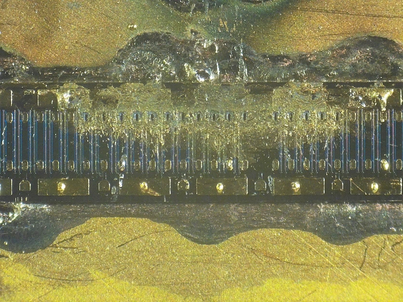
Inspection of this packaged 200W GaN device reveals four main pieces:  two bare GaN HEMT die and two die for impedance matching.  These parts are mounted using conductive die-attach with good thermal properties and are connected using bondwires (only landings shown).  Technically this can be called a multi-chip hybrid or multi-chip-module (MCM).  The entire assembly has been encapsulated in a plastic overmold to reduce cost at the expense of increased parasitic loss.

RFIC and MMIC development is a complex process and every piece of the device needs to be thoroughly analyzed for electrical and thermal properties along with size and cost.  Echoic is highly experienced in the analysis and design of RF / microwave GaN devices.

After an extended time pushing out a whopping 200W CW RF signal, this GaN HEMT transistor decided to call it quits! As the brother of the transistor we last posted (not the exact same device) it saw some real action but soon became a burnt transistor 🙁

We’re showing the bottom mounting plate with the toasted bare die as well as an underside view of the top encapsulation mirrored over. One side has burned out before the other in this “gemini” package. Unlike the ceramic packaged breed, there is no soot and the bondwires were not vaporized. Rather, they have been fossilized into the encapsulation and are poking “into the page” (illustrated). What’s interesting is how much is “captured” inside the mold including an imprint of the GaN die themselves!

Developing high power GaN HEMT power amplifiers and pushing technology to the limits always comes with risks.

Posted on

Will They Mate? – RF Connector and Intermateability Guide

In terms of physical intermateability, many of these RF coaxial connector types do cross-mate without damage.  So if you’re in thinking of purchasing adapters, the matrix below can help you find the right one.

Posted on

What’s Your Type? – RF Coaxial Connector Types

RF Coaxial Connector Types

There are so many types of connectors out there, it would drive any engineering student insane.

Hopefully, we can clear this up.  There are seven main RF connectors used in test and measurement setups:

N     DC-18 GHz

APC-7     DC-18 GHz

SMA     DC-18 GHz

3.5 mm     DC-26.5 GHz

2.92 mm     DC-40 GHz

2.4 mm     DC-50 GHz

1.85 mm     DC-67 GHz

1.0 mm     DC-110 GHz

Coming Soon


Posted on Leave a comment

5G – The Future of Cellular

The complexity of the cellular infrastructure has evolved from 2G to LTE and now 5G.  The expected 5G speeds reaching 1000x that of LTE will not only enhance existing telecom services, but also lay a new infrastructure for emerging applications such as virtual/augmented reality, self-driving cars, the internet of things (IoT) and wearable and implantable devices [1-2].

The 5G architecture will employ multiple input multiple output (MIMO) and beamforming technology to direct signal power for increased over-the-air data rates.  A number of demonstration 5G systems achieving more than 3Gb/s have been published in the literature [2-3].  These MIMO architectures will stimulate new design goals on the size and capabilities of the RF transceiver hardware.  A block diagram of a digital beamforming 5G massive MIMO architecture is shown in Fig. 1.

Several key directions for 5G have emerged.  First, the critical allocation of spectrum will dictate the design and implementation of transceiver hardware.  Due to the highly congested sub-6-GHz cellular bands, mm-Wave frequencies are necessary for achieving the desired low-latency, high speed transmission.  The FCC has approved of several bands for leading cellular carriers including 28GHz (Verizon, AT&T, T-Mobile), 37GHz and 39GHz (T-Mobile) [4].  Initial development at 28GHz is the most likely but still has significant challenges.  While full mm-wave 5G infrastructure is being developed, carriers will first implement sub-6GHz 5G systems employing many of the same MIMO beamforming techniques but at lower, more technologically accessible frequencies.  A number of sub-6GHz 5G MIMO systems have been demonstrated at 3.3-4.2 GHz [5].

Massive MIMO beamforming will require a multiplicity of RF circuitry for each antenna element in the phased-array transceiver system.  Therefore, size, cost and power density are crucial figures of merit for both the base station and handset architectures.  Analog, digital and hybrid beamforming techniques are under consideration.  A multiplicity of RF transmit and receive chains will be required as shown in Fig. 1.

Fig. 1. Digital beamforming architecture for 5G massive MIMO systems.

References

  1. Ericsson, Stockholm, Sweden, “5G systems,” 2017. [Online]. Available: https://www.ericsson.com/res/docs/whitepapers/wp-5g-systems.pdf
  2. Gozalvez, “Samsung Electronics Sets 5G Speed Record at 7.5 Gb/s,” IEEE Vehicular Technology Magazine, Feb 2015, pp. 12-16.
  3. Sadhu, Y. Tousi, J. Hallin et al., “A 28GHz 32-Element Phased-Array Transceiver IC with Concurrent Dual Polarized Beams and 1.4 Degree Beam-Steering Resolution for 5G Communication,” 2017 IEEE Solid-State Circuits Conference, Feb 2017.
  4. 5gamericas, Bellevue, WA, “5G Spectrum Recommendations,” 2015. [Online]. Available: http://www.5gamericas.org/files/6514/3930/9262/4G_Americas_5G_Spectrum_Recommendations_White_Paper.pdf
  5. Goovaerts, “Intel Unveils 5G Modem with Support for Sub-6 GHz, 28 GHz at CES,” [Online]. Available: https://www.wirelessweek.com/news/2017/01/intel-unveils-5g-modem-support-sub-6-ghz-28-ghz-ces
  6. Wolfspeed, “GaN HEMT MMICs,” Accessed April 2017. [Online]. Available: http://www.wolfspeed.com/rf/foundry-services/gan-hemt-mmic
  7. Global Comm. Semi., “GaAs & GaN RF Technologies,” Accessed April 2017. [Online]. Available: http://www.gcsincorp.com/dedicated_pure-play_wafer_foundry/GaAs%20&%20GaN%20RF%20Technologies.php
  8. Northrop Grumman Corp., “Gallium Nitride (GaN) HEMT for High-Power, High-Frequency Electronics,” Accessed April 2017. [Online]. Available: http://www.northropgrumman.com/BusinessVentures/Microelectronics/Products/Pages/Gallium-Nitride-(GaN)-HEMT.aspx
  9. Ommic, “Technology,” Accessed April 2017. [Online]. Available: http://www.ommic.com/site/tech-2
  10. Qorvo, “Gallium Nitride (GaN), GaN: The Industry’s Hot Technology,” Accessed April 2017. [Online]. Available: http://www.qorvo.com/innovation/technology/gan
  11. National Research Council Canada, “GaN Design Kits,” Accessed April 2017. [Online]. Available: http://www.nrc-cnrc.gc.ca/eng/solutions/advisory/gan_design_kit/index.html
  12. UMS, “Foundry Services,” Accessed April 2017. [Online]. Available: http://www.ums-gaas.com/telechargement/1606_Brochure_Foundry_2016.pdf
  13. S. Yuk, G. R. Branner, and D. J. McQuate, “A Wideband, Multiharmonic Empirical Large-Signal Model for High-Power GaN HEMTs With Self-Heating and Charge-Trapping Effects, IEEE Trans. MTT, vol. 57, no. 12, pp. 3322-3332, Dec. 2009.
  14. -S. Noh, Y.-H. Choi, I. Yom, “Ka-band GaN power amplifier MMIC chipset for satellite and 5G cellular communications,” 2015 IEEE 4th Asia-Pacific Conference on Antennas and Propagation (APCAP), June 2015.
  15. Northrop Grumman, West Falls Church, VA , “APN228 27-31 GHz GaN Power Amplifier Datasheet Revision: April 2015,” Apr. 2015. [Online]. Available: http://www.northropgrumman.com/BusinessVentures/Microelectronics/Products/Documents/pageDocs/APN228rev0415.pdf
  16. Micovic; D. F. Brown; D. Regan; J. Wong; Y. Tang; F. Herrault; D. Santos; S. D. Burnham; J. Tai; E. Prophet; I. Khalaf; C. McGuire; H. Bracamontes; H. Fung; A. K. Kurdoghlian; A. Schmitz, “High frequency GaN HEMTs for RF MMIC applications,” 2016 IEEE International Electron Devices Meeting (IEDM), Dec. 2016.
  17. Kallfass, G. Eren, R. Weber, S. Wagner, D. Schwantuschke, R. Quay and O. Ambacher, “High linearity active GaN-HEMT down-converter MMIC for E-band radar applications,” 2014 Euro. Microw. Int. Circ. Conf., Oct. 2014, pp. 128-131.
  18. M-N. Do, M. Seelmann-Eggebert, R. Quay, D. Langrez, J-L. Cazaux, “AlGaN/GaN mixer MMICs, and RF front-end receivers for C-, Ku-, and Ka-band space applications,” 2010 Euro. Microw. Int. Circ. Conf., Sept. 2010, pp. 57-60.
  19. van Heijningen, J.A. Hoogland, A.P. de Hek, F.E. van Vliet, “6-12 GHz Double-Balanced Image-Reject Mixer MMIC in 0.25um AlGaN/GaN Technology,” Proc. Of 9th Euro. Microw. Int. Cir. Conf., Oct. 2014.
  20. Henderson, E. Camargo, Microwave Mixer Technology and Applications, Artech House, Jul. 2013.
  21. -Y. Wong, W. Chen, Q. Zhou and K. J. Chen, “Zero-Bias Mixer Based on AlGaN/GaN Lateral Field-Effect Diodes for High-Temperature Wireless Sensor and RFID Applications,” IEEE. Trans. On Electron Dev., Vol. 56, No. 12, Dec. 2009, pp. 2888-2894.
  22. Polli, M. Palomba, S. Colangeli, M. Vittori, E. Limiti, “High power-handling GaN switch for S-band applications,” Integrated Nonlinear Microw. and Millimetre-Wave Circuits Workshop, Apr. 20-21, 2017.
  23. Bunz, R. Reber, P. Schuh, M. Oppermann, “High power broadband GaN switch MMICs,” Microwave Integrated Circuits Conference (EuMIC), Sept 2015.
  24. Cory and D. Fryklund, “Solid State RF/Microwave Switch Technology: Part 2,” Accessed June 2017. [Online]. Available: http://www.skyworksinc.com/downloads/press_room/published_articles/MPD_062009.pdf
  25. Analog Devices, “HMC547LC3 GaAs SPDT Non-reflective Switch, DC-28GHz,” Accessed June 2017. [Online]. Available: http://www.analog.com/media/en/technical-documentation/data-sheets/hmc547lc3.pdf
  26. Peregrine Semiconductor, “PE42525 UltraCMOS SPDT RF Switch, 9kHz-60GHz,” Accessed June 2017. [Online]. Available: http://www.psemi.com/pdf/datasheets/pe42525ds.pdf
  27. S. Yuk, G. R. Branner, and C. Wong, “High Power, High Conversion Gain Frequency Doublers using SiC MESFETs and AlGaN/GaN HEMTs,” in IEEE MTT-S Int. Microw. Symp. Dig., pp. 1008-1011, May 2010.